DenseLight provides one-stop design and manufacturing solutions
source:laserfair.com
keywords: denselight
Time:2019-11-18
DenseLight provides one-stop design and manufacturing solutions, ranging from Integrated Photonics Platforms, design and simulation, epitaxial growth, wafer fabrication, chip production, in-line optical coating, sub-mounting, photonic measurements to product tests and screening.Engineering, Testing and Manufacturing are housed in a 15,000 sq. ft. clean room that features fully equipped vertically integrated volume manufacturing from wafer fabrication to test and packaging. DenseLight processes Indium Phosphide (InP) and Gallium Arsenide (GaAs) based optoelectronic devices and photonic integrated circuits there. Our technology and development business processes enable us to work with companies at various stages of their product lifecycle. We become embedded partners in projects, delivering on-time value solutions that are faster and cost competitive for photonic applications.
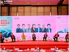 GBA High-Standard Summit Addresses Four AI+Laser Welding Core Propositions
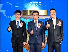 Three Co-founders of a Leading Domestic LiDAR Maker Co-found a Robotics Firm
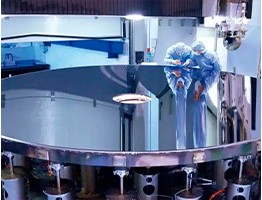 High-Efficiency Conversion Feeds R&D! Optoelectronic HOPE Model Builds a New Industrial Engine
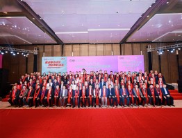 Four-Meeting Linkage: China Laser CEO Shenzhen Night Shines Bright
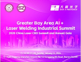 Lead the Intelligent Welding Revolution: Greater Bay Area AI + Laser Welding Summit
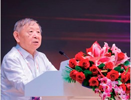 Father of Shenguang Facility: Building Three Generations of National Strategic Equipment
 LASERVALL's Li Mengmeng: A Leader in Laser Solder Ball Welding, Deep in Automated Niche Sectors
 Intelligent Scientific Systems: Leading Domestic Ultrafast Imaging, Redefining Visual Perception
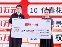 From Rural Girl to Laser Helmsman: Fu Chunhua's Light-Chasing Journey
 Scanner Optics: Galvanometer Tech Leader